Search results
Search for "scan speed" in Full Text gives 43 result(s) in Beilstein Journal of Nanotechnology.
Graphene removal by water-assisted focused electron-beam-induced etching – unveiling the dose and dwell time impact on the etch profile and topographical changes in SiO2 substrates
Beilstein J. Nanotechnol. 2024, 15, 190–198, doi:10.3762/bjnano.15.18

- analysis. Thus, the graphene could be modified and immediately measured by AFM without changing the environment. The analysis was performed by using the tapping mode and the Akiyama probe (Nanosensors). Data shown in Figure 4 were measured with the following parameters: scan speed of 20 µm/m, scan range of


Enhanced feedback performance in off-resonance AFM modes through pulse train sampling
Beilstein J. Nanotechnol. 2024, 15, 134–143, doi:10.3762/bjnano.15.13

- force, as well as reduced lateral force. Simultaneously, they enable mechanical property mapping of the sample. However, ORT modes have an intrinsic drawback: a low scan speed due to the limited ORT rate, generally in the low-kilohertz range. Here, we analyze how the conventional ORT control method
- to these modes (that tap on the surface at a frequency far from the cantilevers’ resonance frequency) from now on in this manuscript generically as off-resonance tapping (ORT) modes. Despite its many benefits, ORT has the drawback of limited scan speed, which stems from the frequency of actuation and
- mode, resulting in increased lateral forces. Therefore, a trade-off between the scan speed and lateral force needs to be considered. The bandwidth of the Z actuator is the other factor that limits the achievable improvement with the pulse sampling method. To fully benefit from multiple closed-loop


Assessing phytotoxicity and tolerance levels of ZnO nanoparticles on Raphanus sativus: implications for widespread adoptions
Beilstein J. Nanotechnol. 2024, 15, 115–125, doi:10.3762/bjnano.15.11

- (Rigaku Ultima IV X-ray Diffractometer) with Cu Kα radiation (1.54059292 Å) over a 2θ range of 20–80° with a scan speed of 2° min−1 at 30 mA and 40 kV [25]. The chemical nature and molecular bonding of the synthesized sample were studied using FTIR (Bruker Vertex80 FT-IR Spectrometer) at a range of 400


A multi-resistance wide-range calibration sample for conductive probe atomic force microscopy measurements
Beilstein J. Nanotechnol. 2023, 14, 1141–1148, doi:10.3762/bjnano.14.94

- -AFM measurements in scanning mode. To extract quantitative values comparable to those listed in Table 1, the surface of each electrode was individually imaged at different locations using the same operating parameters, that is, scan speed, scan orientation, applied force, and bias voltage. A histogram


Industrial perspectives for personalized microneedles
Beilstein J. Nanotechnol. 2023, 14, 857–864, doi:10.3762/bjnano.14.70

- printers (e.g., Nanoscribe Quantum X platforms) producing polymer masters. The increased scan speed and throughput are the result of new supporting technologies coming to market, such as replacing piezoelectric stages with galvanometric mirrors. These new technologies continue to decrease the gap in


On the use of Raman spectroscopy to characterize mass-produced graphene nanoplatelets
Beilstein J. Nanotechnol. 2023, 14, 509–521, doi:10.3762/bjnano.14.42

- Research, Oxford Instruments, UK). AFM images were recorded using Si AFM probes (MikroMasch HQ:NSC15, 40 N/m, 325 kHz, MikroMasch, Bulgaria) in tapping-mode feedback. AFM images were measured in square areas between 6 μm × 6 μm and 8 μm × 8 μm using 1024 × 1024 pixels with a scan speed below 20 μm·s−1. To


An atomic force microscope integrated with a helium ion microscope for correlative nanoscale characterization
Beilstein J. Nanotechnol. 2020, 11, 1272–1279, doi:10.3762/bjnano.11.111

- very slow in vacuum [29]. In ORT, the tapping rate is a least one order of magnitude below the first resonance of the cantilever and hence the enhancement of the Q-factor in vacuum is less detrimental to the achievable scan speed. Results The system has been experimentally tested on a variety of sample


Wet-spinning of magneto-responsive helical chitosan microfibers
Beilstein J. Nanotechnol. 2020, 11, 991–999, doi:10.3762/bjnano.11.83

- obtained at a magnetic field strength of 40 × 103 Gs using 72 points per loop with a scan speed of 10 s per point. The range covered during the hysteresis scan was between +22 × 103 Oe and −22 × 103 Oe. During the scans, the magnetic field was measured with a FCM-10 control module and the magnetization


Nickel nanoparticles supported on a covalent triazine framework as electrocatalyst for oxygen evolution reaction and oxygen reduction reactions
Beilstein J. Nanotechnol. 2020, 11, 770–781, doi:10.3762/bjnano.11.62

- ° and 100° 2θ with a scan speed of 2 s/step and 0.057° (2θ) step size. Nitrogen sorption measurements were performed with a Nova 4000e from Quantachrome at 77 K and evaluated with the NovaWin 11.03 software. The materials were first degassed under vacuum (<10−2 mbar) at 120 °C overnight. The Brunauer


Comparison of fresh and aged lithium iron phosphate cathodes using a tailored electrochemical strain microscopy technique
Beilstein J. Nanotechnol. 2020, 11, 583–596, doi:10.3762/bjnano.11.46

- 2a. It indicates that the signal is not influenced by the topography of the sample, since the flat locations in the top and bottom of the image show a distinct ESM signal. Additionally, due to the slow scan speed of 0.2 Hz, we assume a stable tip–sample contact during the measurement. Considering


Fabrication and characterization of Si1−xGex nanocrystals in as-grown and annealed structures: a comparative study
Beilstein J. Nanotechnol. 2019, 10, 1873–1882, doi:10.3762/bjnano.10.182

- ° divergence slit and a 0.27° parallel plate collimator was used. The measurement run was made over 0.005 °/s scan speed. For photoconductive measurement, Al contacts (1 × 4 mm2) in co-planar geometry with a gap of 4 mm between them were deposited by evaporation. A schematic of the photocurrent setup and the


Development of a new hybrid approach combining AFM and SEM for the nanoparticle dimensional metrology
Beilstein J. Nanotechnol. 2019, 10, 1523–1536, doi:10.3762/bjnano.10.150

- working distance set at 2 mm). All others scan parameters, including pixel size, scan speed, contrast, and brightness, are fixed for all images. The pixel size was set to 1.4 nm with a total cycle time to record an image of 28.4 s. The values assigned for contrast and brightness were 31.4% and 49
- -vibration table. The pixel size was set to 5.0 nm for all AFM measurements. Moreover, the scanning parameters are fixed regardless of the NP population under study. The scan speed is equal to 4 µm/s with constant PID parameters set at 0.8 for integral gain and 10 for the proportional one. Laboratory


Rapid thermal annealing for high-quality ITO thin films deposited by radio-frequency magnetron sputtering
Beilstein J. Nanotechnol. 2019, 10, 1511–1522, doi:10.3762/bjnano.10.149

- ) with Cu Kα radiation (λ = 1.5418 Å) at a power of 40 kV/40 mA. The scan was performed between 20° and 60° with a 2 s/step scan speed and 0.04° step. Optical transmission spectra of the deposited thin films were measured with a UV–vis–NIR Perkin Elmer 950 spectrophotometer (190–3300 nm). The electrical


Growth of lithium hydride thin films from solutions: Towards solution atomic layer deposition of lithiated films
Beilstein J. Nanotechnol. 2019, 10, 1443–1451, doi:10.3762/bjnano.10.142

- scan speed was changed as necessary. Ellipsometry measurements were performed using SENTECH SENpro ellipsometer, using the included halogen lamp. Frequency measurements on a quartz crystal were performed in situ using an OpenQCM module at 10 MHz. Results and Discussion Structure and possible reaction
- the films started reacting with air. GIXRD of as-deposited samples with indexed reflections attributed to cubic LiH. GIXRD was performed at an incidence angle of 1°, and a scan speed 0.02°per 14.5 seconds. Possible mechanism of the surface reactions. Derivative Auger spectra confirming the presence of


Imaging the surface potential at the steps on the rutile TiO2(110) surface by Kelvin probe force microscopy
Beilstein J. Nanotechnol. 2019, 10, 1228–1236, doi:10.3762/bjnano.10.122

- the probe was correct. In the experiment, even though the scan speed changed, the height of the step edges remained constant, indicating that the height of the step was not affected by a potential non-linear response of the z-piezo actuator. Thus, the observed steps of 200 pm height must be monatomic

![[Graphic 16]](/bjnano/content/inline/2190-4286-10-122-i16.svg?max-width=637&scale=1.18182) and
and ![[Graphic 17]](/bjnano/content/inline/2190-4286-10-122-i17.svg?max-width=637&scale=1.18182) .
.


![[Graphic 38]](/bjnano/content/inline/2190-4286-10-122-i38.svg?max-width=637&scale=1.18182) and
and ![[Graphic 39]](/bjnano/content/inline/2190-4286-10-122-i39.svg?max-width=637&scale=1.18182) steps. (a) Topographic image...
steps. (a) Topographic image...


![[Graphic 72]](/bjnano/content/inline/2190-4286-10-122-i72.svg?max-width=637&scale=1.18182) , b)
, b) ![[Graphic 73]](/bjnano/content/inline/2190-4286-10-122-i73.svg?max-width=637&scale=1.18182) , c) reduced
, c) reduced ![[Graphic 74]](/bjnano/content/inline/2190-4286-10-122-i74.svg?max-width=637&scale=1.18182) , and d)
, and d) ![[Graphic 75]](/bjnano/content/inline/2190-4286-10-122-i75.svg?max-width=637&scale=1.18182) steps. B...
steps. B...
Influence of dielectric layer thickness and roughness on topographic effects in magnetic force microscopy
Beilstein J. Nanotechnol. 2019, 10, 1056–1064, doi:10.3762/bjnano.10.106

- increase the signal-to-noise ratio. The resolution of the images is 254 measuring points per line, and the scan speed is 0.9 Hz. The force gradient is detected by phase shifts in interleave mode. A magnetic ASYMFM-HM tip was used for all measurements in order to assure a high magnetic sensitivity. The


![[Graphic 2]](/bjnano/content/inline/2190-4286-10-106-i7.svg?max-width=637&scale=1.18182) ; black line) and measured phase shift for single nanoparticles with 10 ± 2 nm diameter...
; black line) and measured phase shift for single nanoparticles with 10 ± 2 nm diameter...


Charged particle single nanometre manufacturing
Beilstein J. Nanotechnol. 2018, 9, 2855–2882, doi:10.3762/bjnano.9.266


Biomimetic surface structures in steel fabricated with femtosecond laser pulses: influence of laser rescanning on morphology and wettability
Beilstein J. Nanotechnol. 2018, 9, 2802–2812, doi:10.3762/bjnano.9.262

- porous structure in combination with oxidation, mediated by the high temperature reached over a long time, as a consequence of the slow scan speed and high fluence. This interpretation is supported by the brownish color of the surface that can be realized upon inspection. Somewhat similar results have
- fabricated in steel, with the experimental parameters given in Table 1, arranged according to increasing laser fluence and number of scans. The total fabrication time for all the areas was kept constant by adjusting the scan speed and repetition rate accordingly. For all structure types, the characteristic


Enhanced antineoplastic/therapeutic efficacy using 5-fluorouracil-loaded calcium phosphate nanoparticles
Beilstein J. Nanotechnol. 2018, 9, 2499–2515, doi:10.3762/bjnano.9.233

- diffractometer using Ni-filtered Cu Kα radiation with a typical scan speed of 0.05 °/min in the range of 2θ = 5–90°. Transmission electron microscopy The surface and internal morphology as well as the size of CaP@5-FU NPs were visualised by TEM. A small drop of the aqueous dispersed CaP@5-FU NPs with the


Scanning speed phenomenon in contact-resonance atomic force microscopy
Beilstein J. Nanotechnol. 2018, 9, 945–952, doi:10.3762/bjnano.9.87

- /bjnano.9.87 Abstract This work presents data confirming the existence of a scan speed related phenomenon in contact-mode atomic force microscopy (AFM). Specifically, contact-resonance spectroscopy is used to interrogate this phenomenon. Above a critical scan speed, a monotonic decrease in the recorded
- contact-resonance frequency is observed with increasing scan speed. Proper characterization and understanding of this phenomenon is necessary to conduct accurate quantitative imaging using contact-resonance AFM, and other contact-mode AFM techniques, at higher scan speeds. A squeeze film hydrodynamic
- theory is proposed to explain this phenomenon, and model predictions are compared against the experimental data. Keywords: atomic force microscope; contact resonance; liquid; phenomenon; scan speed; Introduction With the rise in popularity of simultaneous topographic imaging and material property


A robust AFM-based method for locally measuring the elasticity of samples
Beilstein J. Nanotechnol. 2018, 9, 1–10, doi:10.3762/bjnano.9.1

- × 2.5 μm were scanned at a resolution of 256 × 256 pixels and a scan speed of 2 μm·s−1. Cantilevers The measurements were performed with a PPP-CONT cantilever from NanosensorsTM (Si tip of Young’s modulus Etip ≈ 169 GPa) characterized by f0,1 = 16.35 kHz, k1 = 0.324 N·m−1, Q1 = 68, f0,2 = 102.98 kHz, k2


Fixation mechanisms of nanoparticles on substrates by electron beam irradiation
Beilstein J. Nanotechnol. 2017, 8, 1523–1529, doi:10.3762/bjnano.8.153

- scattering in the substrate. The backscattering ranges were theoretically analyzed for several materials at various electron energies by Kanaya [9], and the results agree well with our MC results. The effects of electron-beam conditions including accelerating voltage and beam scan speed, obtained by
- experiments, are summarized in Figure 7. The width increases greatly with increasing accelerating voltage. An increase in width with decreasing scan speed is reasonable because the number of irradiating electrons per unit area increases. To achieve thin lines, decreasing the accelerating voltage and
- increasing the scan speed are thus effective. Figure 8a shows a line of particles produced at an accelerating voltage of 1.5 kV and a scan speed of 1.4 μm/s, resulting in a line width of about 0.13 μm. Figure 8b shows a spiral pattern of a particle line demonstrating the flexibility of this technique. Effect


Ion beam profiling from the interaction with a freestanding 2D layer
Beilstein J. Nanotechnol. 2017, 8, 682–687, doi:10.3762/bjnano.8.73

- focused ion beam across the knife edge can change the edge shape because of a milling effect incurred by the ion beam irradiation itself. Increasing the scan speed over the edge in order to avert the damage, gives rise to other problems such as shot noise and statistical beam fluctuations. Another


Carbon nanotube-wrapped Fe2O3 anode with improved performance for lithium-ion batteries
Beilstein J. Nanotechnol. 2017, 8, 649–656, doi:10.3762/bjnano.8.69

- ) Discharge–charge profiles of COOH-MWCNT at a current density of 500 mA·g−1; (b) discharge–charge profiles of Fe2O3/COOH-MWCNT composites at a current density of 500 mA·g−1; (c) cyclic voltammograms of COOH-MWCNT at a scan speed of 0.05 mV·s−1; (d) cyclic voltammograms of Fe2O3/COOH-MWCNT at a scan speed of


Noise in NC-AFM measurements with significant tip–sample interaction
Beilstein J. Nanotechnol. 2016, 7, 1885–1904, doi:10.3762/bjnano.7.181
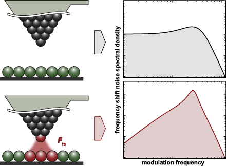
- always the experimental task defining the desired spatial resolution λ that is, for instance, a fraction of the atomic periodicity in atomic resolution imaging, and the available time for the measurement expressed by the scan speed vscan. Assuming perfectly band-limited output signals, the sampling
- theorem requires the product of scan speed and inverse spatial resolution to be smaller than half of the detection bandwidth ΔfBW, or This often requires a compromise as using the optimum bandwidth defined by operation at the thermal noise limit [11] may impose a scan speed that is not practical


![[Graphic 32]](/bjnano/content/inline/2190-4286-7-181-i73.png?max-width=637&scale=1.18182) wit...
wit...

![[Graphic 34]](/bjnano/content/inline/2190-4286-7-181-i75.png?max-width=637&scale=1.18182) wit...
wit...


